Core Board Introduction
Product Overview
This core board is based on the Qualcomm QCS8550, a flagship SoC for high-end edge AI and smart terminals. The QCS8550 integrates a hexa-core Kryo CPU, Adreno 740 GPU, 48 TOPS NPU, 8K VPU, and Spectra ISP, purpose-built for high-compute, high-stability scenarios such as robotics, industrial AI, high-end IPC/VR, and automotive applications.
This core board features strict material selection and design for ultra-slim applications. Its compact dimensions and rich interfaces facilitate integration into finished products, and it can be used in digital signage, interactive touch, consumer electronics, entertainment systems, and other industries.
Product Appearance
SOM8550 core board physical photos:
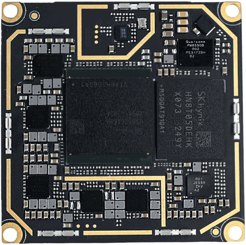
Front
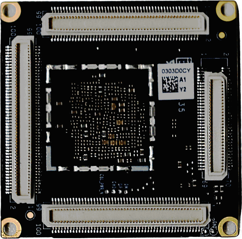
Back
Physical Dimensions
| Item | Parameter |
|---|---|
| PCBA Dimensions | 40 mm × 40 mm (±0.5 mm) |
| Board Thickness | 1.0 mm (±10%) |
| Mounting Hole Diameter | 4 mm |
| Screw Hole Spec | ∮2.2 mm × 4 (±10%) |
For detailed dimensional information, contact APLUX FAE at support@aidlux.com.
Specifications
CPU
The core board uses Qualcomm QCS8550 CPU in 1581 MPSP package, chip dimensions 15.6 × 14.0 × 0.56 mm.
| Item | Parameter |
|---|---|
| AI Performance | 48 TOPS (INT8) |
| CPU | 1× Kryo Prime @ 3.2 GHz + 2× Kryo Gold @ 2.8 GHz + 3× Kryo Silver @ 2.0 GHz |
| GPU | Adreno 740 |
| Process | 4 nm |
| Video Decode | 4K@240 fps / 8K@60 fps (H.264 / H.265 / VP9) |
| Video Encode | 4K@120 fps / 8K@30 fps (H.264 / H.265) |
ROM
The core board's UFS interface supports up to UFS 4.0 Gear 5 Rate A, 1×2 lane. Default onboard is a single SK Hynix 128 GB UFS, expandable up to 512 GB.
RAM
The core board connects to LPDDR5X via EBI controller in PoP form factor, with a maximum frequency of 4266 MHz. Default onboard is 12 GB LPDDR5X, expandable up to 24 GB.
Power
The core board uses Qualcomm PMIC power solution to meet system power and CPU power-up/down sequencing requirements. It uses DC power with a typical supply voltage of 3.8 V.
Peripheral Resource Overview
The core board exposes the following interface resources via board-to-board connectors (Panasonic AXK600337YG / AXK680337YG series):
| Interface Resource | Quantity | Performance Parameters |
|---|---|---|
| CSI | 5 groups | 4 groups 4-lane + 1 group 2-lane, DPHY V1.2 2.5 Gbps/lane, CPHY v2.0 13.68 Gbps/trio |
| DSI | 2 groups | Two groups 4-lane, up to 3480×2160@120 Hz, 3360×1600@144 Hz |
| PCIe | 2 groups | 1× PCIe 3.0 2-lane (8 Gbps) + 1× PCIe 4.0 2-lane (16 Gbps) |
| USB | 1 group | USB 3.1 Gen2, up to 10 Gbps, supports OTG, DP1.4 compatible, supports MST mode |
| SD | 1 group | 4-bit, supports SD 3.0 / SDR104, 1.2 V IO level only |
| SPI | 5 groups | 4 groups general-purpose SPI + 1 group dedicated SPI, master mode only |
| UART | 10 groups | 1 group debug + 1 group 4-wire + 8 groups 2-wire |
| I2C | 9 groups | 4 groups camera-dedicated I2C + 4 groups general-purpose I2C + 1 group sensor I2C |
| I2S | 2 groups | 1 group non-LPI I2S + 1 group LPI I2S |
| SWR | 1 group | Supports PCM / PDM / DATA data formats |
| GPIO | 50 groups | 50 GPIO resources |
| ADC | 2 groups | Voltage range 0–1.875 V, sampling rate 4.8 MHz |
| PWM | 2 groups | Derived from PM8550 |
Important Notes
Please observe the following key notes when assembling and using the A8550MA1 SOM module:
- Environmental requirements: Relative humidity 0–95% non-condensing, operating temperature -25°C ~ +50°C, storage temperature -40°C ~ +85°C.
- ESD protection: This product does not have built-in ESD protection. ESD protection must be designed on the carrier board.
- Voltage level matching: Pay attention to voltage level matching when designing external interfaces.
- High-speed signals: When designing high-speed signal interfaces, follow design guidelines for layout routing to ensure interface performance.
Document Information
- Official product name: A8550MA1 SOM Module
- Full product code: A8550MA1
- Document version: V1.0
- Release date: 2026-06-11
- Classification: Public
- Applicable scope: A8550MA1 SOM module and carrier board / product development projects based on this module
© 2026 Chengdu APLUX Intelligence Technology Ltd. Unauthorized reproduction, distribution, or use beyond the scope specified in this document is prohibited without written permission.