Interface Definition
A8625MY1 exposes all interfaces through the Mini PCIe edge connector, including power, data, control, and debug interfaces.
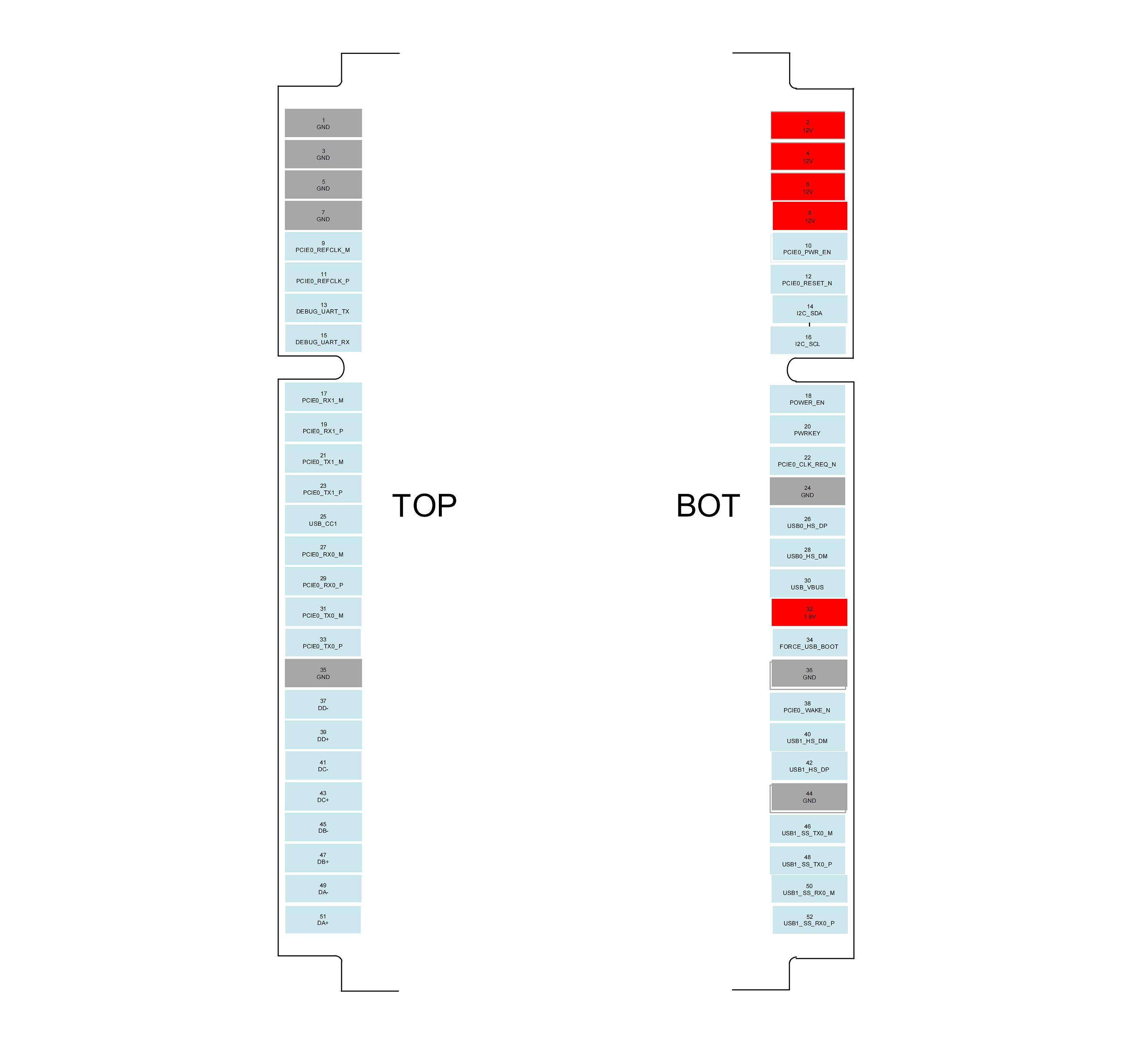
- Interface summary:
| Interface Type | Specification and Function |
|---|---|
| Power Input | 5V~18V wide-voltage input (VCC_IN, Pin 2/4/6/8) |
| Data Interface | 1x2.5Gbps RJ45 Ethernet, 1xPCIe RC Gen3 (2 lane) |
| USB Interface | 1xUSB 3.1 (SuperSpeed), 1xUSB 2.0 (HighSpeed) |
| Control Interface | 1xUART (1.8V, debug serial), 1xI2C (1.8V) |
- Key pin definitions:
| Pin Name | Pin No. | I/O | Description |
|---|---|---|---|
| VCC_IN | 2, 4, 6, 8 | PI | Four input power pins, supports 5~18V wide-voltage supply. Add large capacitors and Zener diodes externally for surge protection. |
| 1.8V-OUT | 32 | PO | 1.8V power output, 100mA. Output is available only after power-on. |
| GND | 1, 3, 5, 7, 35, 24, 36, 44 | - | Ground |
| PCIE0_REFCLK_M | 9 | AO | PCIe reference clock - |
| PCIE0_REFCLK_P | 11 | AO | PCIe reference clock + |
| PCIE0_PWR_EN | 10 | DO | PCIe peripheral power enable, 1.8V level |
| PCIE0_RESET_N | 12 | DO | PCIe reset signal, 1.8V level |
| PCIE0_WAKE_N | 38 | DI | PCIe wake interrupt request signal, 1.8V level |
| PCIE0_CLK_REQ_N | 22 | DI | PCIe clock request signal, 1.8V level |
| PCIE0_RX0_M | 27 | AI | PCIe Lane0 RX - |
| PCIE0_RX0_P | 29 | AI | PCIe Lane0 RX + |
| PCIE0_TX0_M | 31 | AO | PCIe Lane0 TX - |
| PCIE0_TX0_P | 33 | AO | PCIe Lane0 TX + |
| PCIE0_RX1_M | 17 | AI | PCIe Lane1 RX - |
| PCIE0_RX1_P | 19 | AI | PCIe Lane1 RX + |
| PCIE0_TX1_M | 21 | AO | PCIe Lane1 TX - |
| PCIE0_TX1_P | 23 | AO | PCIe Lane1 TX + |
| DD- | 37 | AI/AO | RJ45 differential signal, supports 2.5G and backward compatible with 100M/1000M |
| DD+ | 39 | AI/AO | RJ45 differential signal |
| DC- | 41 | AI/AO | RJ45 differential signal |
| DC+ | 43 | AI/AO | RJ45 differential signal |
| DB- | 45 | AI/AO | RJ45 differential signal |
| DB+ | 47 | AI/AO | RJ45 differential signal |
| DA- | 49 | AI/AO | RJ45 differential signal |
| DA+ | 51 | AI/AO | RJ45 differential signal |
| DEBUG_UART_TX | 13 | DO | DEBUG_TX data output, 1.8V level. Default module debug port. |
| DEBUG_UART_RX | 15 | DI | DEBUG_RX data input, 1.8V level. Default module debug port. |
| I2C_SDA | 14 | OD | I2C signal, 1.8V level. Internally pulled up to 1.8V through 2.2K. |
| I2C_SCL | 16 | OD | I2C signal, 1.8V level. Internally pulled up to 1.8V through 2.2K. |
| USB0_HS_DP | 26 | AI/AO | USB 2.0 differential data positive. When high, module USB2.0 switches to pin 26/28. |
| USB0_HS_DM | 28 | AI/AO | USB 2.0 differential data negative. When high, module USB2.0 switches to pin 26/28. |
| VBUS | 30 | DI | USB power input for USB insertion detection. When high, module USB2.0 switches to pin 26/28. |
| USB1_HS_DM | 40 | AI/AO | USB 2.0 differential data negative. When low, module USB2.0 switches to pin 40/42. |
| USB1_HS_DP | 42 | AI/AO | USB 2.0 differential data positive. When low, module USB2.0 switches to pin 40/42. |
| USB1_SS_TX0_M | 46 | AO | USB 3.1 differential TX - |
| USB1_SS_TX0_P | 48 | AO | USB 3.1 differential TX + |
| USB1_SS_RX0_M | 50 | AI | USB 3.1 differential RX - |
| USB1_SS_RX0_P | 52 | AI | USB 3.1 differential RX + |
Note
For carrier-board package dimensions and pin layout details, refer to the A8625MY1 Hardware Design Guide (contact FAE).